| ⭅ Previous (Adding 65816 Hardware) |
(Mind) Uploading a Chip - Intro
Styles of Reverse Engineering
In this article and the next few, we’ll be looking at a system we’ve been building. While it is far from complete, it would allow us to automatically capture the behavior of any digital circuit plugged into it. If you read science fiction, you may know the idea of “mind uploading”.
While that remains science fiction, we believe we can make progress on a simpler but similar problem. Neurons developed naturally, and we don’t currently know how enough about how they work. But humans created transistors and digital logic gates, so we can understand them completely.
Our goal here is to build a “chip uploader”, which can be connected to some digital (integrated) circuit, capture its behavior, and recreate it through simulation.
Before talking about the uploader we’ve built so far, lets step back and see how chip emulators are typically designed today.
Chip emulation today (Industry vs Retrocomputing)
There are two broad categories of chip emulation. In industry, emulation often refers to using simulators to execute the behavior defined in some HDL language like Verilog. Sometimes this uses specially designed emulator sytems like the Cadence Palladium + Protium (in photo below). This is useful when some specification is already in our posession, and we want to make sure it does what we expect.

In the retrocomputing side of emulation, the goal is usually quite different. Rather than start with a specification and see how it behaves, we usually have the reverse. We typically have some working hardware, without any public specification. We would like to document its behavior completely and accurately, so that we can build systems to emulate the behavior of the physical hardware.
We’ll focus on the retrocomputing side of emulation for the rest of the article. This is reverse-engineering, where we start with a working system and try to understand how it works. Reverse engineering is often necessary, since we aren’t always the specification. We’re focused on digital circuits for now, but similar approaches can often be used for understanding the natural world.
Reverse engineering a chip
When reverse-engineering a chip, usually one of these three approaches are taken:
1. Test programs (non-destructive, software)
People write programs to exercise some part of the system, and observe the results of the program. The tests both give us insights into how the physical system works, and also provide a tool to test a developing emulation as it improves in fidelity.
Pros:
- Accessible. Software can be written and shared easily. Retrocomputing communities can collect large suites of test programs to automate testing of future emulators.
Cons:
- Limited visibility. This is sort of like walking in the dark. We only see things when we bump into them. Only a small subset of information about the chip is directly observable from the software side of things.
; Snippet from our controller test rom for the NES
; Read controller state, and update the OAM copy at page 0x02XX.
; strobe
lda #$01
sta CTRL1
lda #$00
sta CTRL1
; now read each bit for the buttons. If set, use palette 1. otherwise palette 0
ldy #$06    ; OAM offset. 2nd slot(4) + 2 for attribute position
ldx #$08    ; Sprite&tile num
...2. Hardware tracing (non-destructive, hardware)
Similar to the above, but instead the chip is observed physically rather than the software level. A famous example is how Andrew “Bunnie” Huang reverse engineered the original xbox, building custom tooling to analyze the data sent in an out of the chip along the bus. The full story of Hacking the Xbox is both very entertaining and very informative, highly recommended.
Pros:
- Richer data capture. Now instead of just seeing what is visible from software, we can see everything that goes in and out of the chip.
Cons:
- “Hardware is hard”. Not only is it harder to reproduce hardware, but designing and dealing with physical imperfects are an inevitable part of designing hardware.
3. Physical disassembly / decapping (destructive, hardware).
On the other extreme are destructive methods. While these destroy the original device, they allow us to peek inside and see how it is physically organized. Since humans created digital circuits, we fully understand how all the components(transistors, gates) work. When looking at the physical organization, we can then reproduce or “capture” these connections digitally, which will allow us to recreate the behavior via software simulation.
For integrated circuits, this is often called “decapping”. The “chip” you see is actually a large, usually plastic package which protects the very delicate semiconductor on the inside. Removing the “cap” lets you see inside.
 (Dirk Oppelt, CC BY-SA 3.0 https://creativecommons.org/licenses/by/2.0, via Wikimedia Commons)
 (Travis Goodspeed, CC BY 2.0 https://creativecommons.org/licenses/by/2.0, via Wikimedia Commons)
 (Pauli Rautakorpi, CC BY 3.0 https://creativecommons.org/licenses/by/3.0, via Wikimedia Commons.)
Pros:
- Very high fidelity. This essentially gives access to the blueprint of the device.
Cons:
- Destructive. Once this approach is performed, the original chip is not functional. This leads to:
- Wasteful. Since the chip is destroyed in the process, it doesn’t easily allow for iteration. If you mess up, you need to get another chip. Especially for rare or costly chips, this isn’t viable.
- Expensive. While the tools used to get inside the chip can be fairly affordable (acids / lasers / routers), the microscopes required to view and capture the insides can be quite expensive.
The Chip Uploader
We believe the best way to progress is through non-destructive capture. We can experiment more rapidly when there is no risk of losing the original. And by looking at things through an information lens, rather than hardware, we can advantage of highly productive processes of software engineering, such as automated testing and revision control.
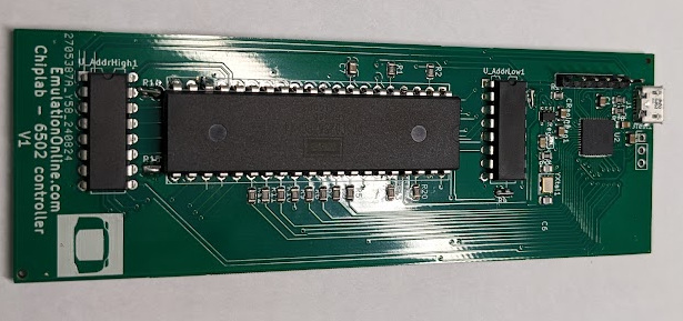
The chiplab we built previously (photo above) is a cross between approaches 1 and 2. You can write arbitrary assembly programs, but then run them against a real chip to observe the behavior. By putting this online, anyone with a web browser can contribute to reverse engineering the 6502 in this way.
There are two main problems with the chiplab as it exists today.
-
We would have to write many programs to exercise and observe all the interesting behavior of the 6502. You can see some of these 6502 test programs and their recorded traces on our github.
-
After capturing this behavior, turning the observations into a functional model (ex: code) is very laborious. Though this hasn’t stopped us, and you can see some examples of this in our 6502 Rust model project, derived from trace behavior.
Given the amount of effort to capture even such a simple chip this way, we’ll need a more efficient process to support more complex systems. We’ve started to make a dent here. This article is already quite long, so we’ll write up more in another article. Make sure to join our newsletter if you’d like to receive an update.
| ⭅ Previous (Adding 65816 Hardware) |